
AlixLabs
Atomic Layer Etching for Nano Device Fabrication
We provide an ALE-based method of manufacturing nanostructures with characteristic size below 20nm.
This is a new method of nanostructure fabrication using the atomic layer etching process, which is inherently a damage-free etch process. Owing to the etching process’s selectivity to inclined surfaces, which has been recently discovered, the inclined surfaces can be used as a mask and in this way walls of tapered structures, which can be readily fabricated by e.g., dry etching or epitaxial growth, will provide masking during the atomic layer etching process. This is why this process provides access to fabrication of extremely small structures in a very precise and efficient way.
Lund
News about AlixLabs

Nanotech Startup AlixLabs Attracts €14M Series A
AlixLabs, a Lund-based deep-tech company building a new generation of semiconductor manufacturing solutions at the below 7 nm scale, has recently announced the successful…
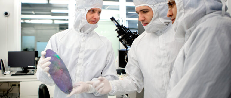
Alix Labs Secures Majority of €10M Investment to Drive AI Processor Development
Lund-based nanotechnology company Alix Labs, led by CEO Jonas Sundqvist, is making strides in developing advanced semiconductor components. Rapidus reports the startup has secured…
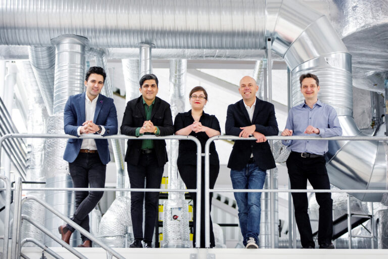
AlixLabs secures over € 3 million investment to advance energy-efficient semiconductor innovation
Swedish semiconductor trailblazer, AlixLabs, has successfully secured over € 3 million (SEK 40 million) in funding to accelerate their pioneering work. Specializing in semiconductor…